Today’s announcement a step in the direction of Act East Policy, as emphasised by Prime Minister of India: Union Minister of Electronics and IT
Three major technologies which will be deployed in this plant are being developed in India: Shri Ashwini Vaishnaw
These indigenous advanced semiconductor packaging technologies to be extremely critical for key applications in automotive, communications, and other sectors
85,000 industry-ready workforce in semiconductor chip design being trained at 113 academic institutions across the country; Nine such institutions in North-east
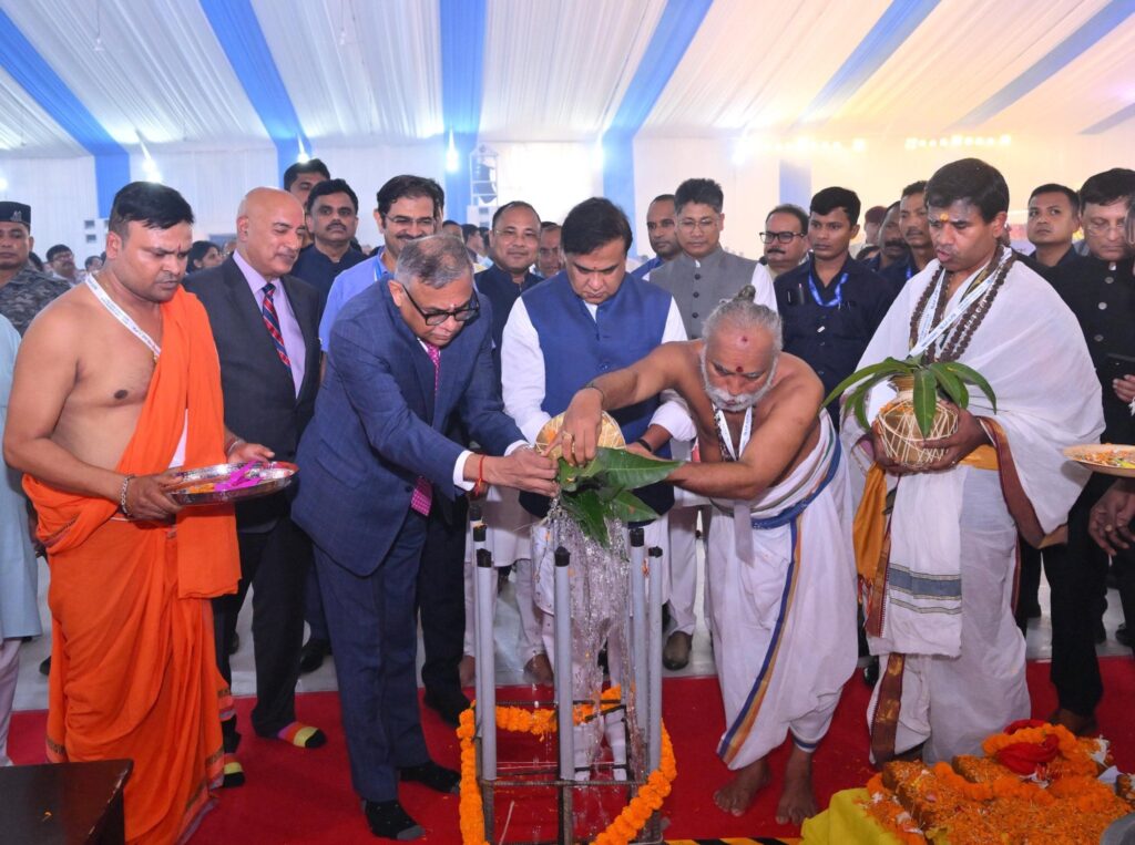
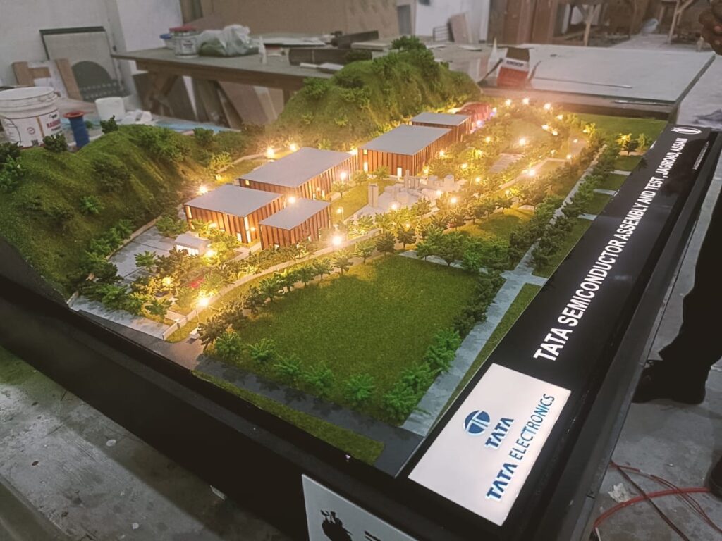
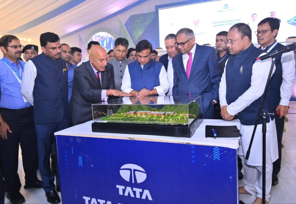
PIB News 3 August 2024 : In a significant step towards creating an end-to-end semiconductor manufacturing ecosystem in India, the function for commencement of construction of Tata’s semiconductor unit in Assam unit was held today in the presence of Hon’ble Chief Minister of Assam, Shri Himanta Biswa Sarma and Chairman of Tata Sons Limited N Chandrasekaran. Later today, the Union Minister for Railways, Electronics & Information Technology and Information and Broadcasting, Sh. Ashwini Vaishnav, during his interaction with the media, stated that the Prime Minister of India has always emphasised on Act East policy and a very important milestone is being achieved today in Assam with the commencement of construction of this facility. He mentioned that this project was approved by the Union Cabinet on 29th February, 2024.

The programme for development of Semiconductors and Display Manufacturing Ecosystem in India was notified on 21.12.2021 with a total outlay of ₹ 76,000 crore. In June, 2023, the Union Cabinet led by Prime Minister of India, Shri Narendra Modi had approved the proposal of Micron for setting up a semiconductor unit in Sanand, Gujarat whose construction is progressing at a rapid pace.
About the semiconductor unit
The Union Minister mentioned that this unit will be set up with an investment of ₹ 27 thousand crores and is expected to generate 15 thousand direct and 11-13 thousand indirect jobs. While highlighting the importance of the Semiconductor industry as being a foundational one, he said that employment opportunities in various upstream and downstream industries will be created.

The proposed capacity of this unit is 4.83 crore semiconductor chips per day. He also pointed out that this unit will be the site for development of indigenous advanced semiconductor packaging technologies including Wire Bond, flip chip and I-SIP (integrated system in package) technologies and all these three major technologies which will be deployed in this plant are being developed in India. These technologies are extremely critical for key applications such as automotive (especially electric vehicles), communications, network infrastructure and others

Talent development plan
The Union Minister also mentioned that 85,000 industry-ready workforce at B.Tech, M.Tech and PhD level in semiconductor chip design are being trained at 113 academic institutions across the country. 9 of these are in North-east, whose details are mentioned below:
Sr. No
State
Name of Institution
1
Assam
National Institute of Technology Silchar
2
Mizoram
National Institute of Technology Mizoram
3
Manipur
National Institute of Technology Manipur
4
Nagaland
National Institute of Technology Nagaland
5
Tripura
National Institute of Technology Agartala
6
Sikkim
National Institute of Technology Sikkim
7
Arunachal Pradesh
National Institute of Technology Arunachal Pradesh
8
Meghalaya
North Eastern Hill University, Shillong
National Institute of Technology Meghalaya
Today’s announcement marks a significant milestone in accelerating the progress of North-East and realizing the Prime Minister of India’s vision of ‘Viksit Bharat, Viksit Northeast’.


